
What is Unijunction Transistor
A unijunction transistor, shorten UJT name called its contains only one junction. It have a three terminal device namely Emitter (E), Base1(B1), Base2(B2). The basic this device and its change are necessary latching switches whose working is to the four layer diode, the most important difference being that the device switching voltage can be easily changed by the circuit manufacture. Such as the four layer diode, this device is usually operated as a switch and finds most frequent applications in oscillators, timing circuits and SCR & TRIAC trigger circuits.
Construction of UJT
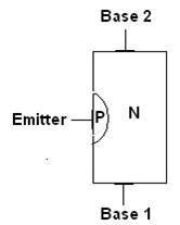
The construction of UJT is consists a lightly doped, N- type silicon material substrate provided with ohmic contact at two ends.UJT three terminal device. It has only PN junction so the namely called unijuction device. It controls a large AC power with small gain, and not be used as amplifier. It exhibits negative resistance characteristics and can be used as an oscillator. The two end one is base-1 (B1), and another one is base-2 (B2). The p region act as an emitter terminal (E). The internal resistance RBB is has between B1 and B2, the resistance range of this 4KΩ and 10kΩ. The internal resistance can be divided into the from terminal B1 to emitter named resistance is RB1. From the terminal B2 to emitter named resistance is RB2. Usually the emitter close resistance RB2 value is 4.2 KΩ or 2.8 KΩ.
Structure of BJT
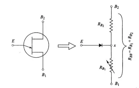
A.symbol equivalent circuit
UJT Triggering (or) line synchronized triggering

Triggering of UJT
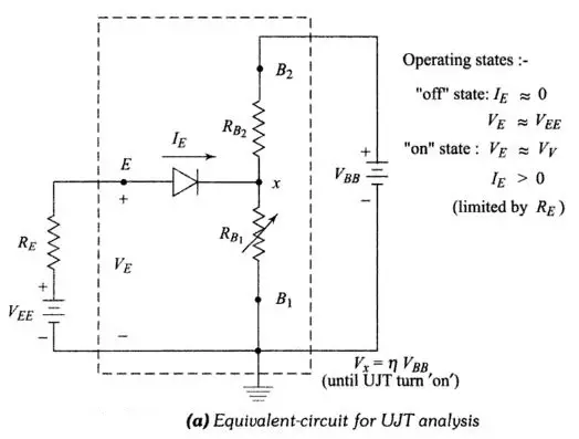
The device emitter terminal (E) to base terminal (B1) connected to V EE , the VBB voltage terminals are connected to device base (B1)and base (B2). The VEE is not a source voltage, base (B1) terminal output get VEE acting as capacitor. The total resistance RBB (RBB=RB1+RB2) is greater than emitter voltage the PN junction diode get reverse bias the device is OFF condition (RBB>E). On other hand RBB is less than the emitter voltage the PN junction diode get forward bias the UJT ON state (RBB< E).
The resistance RB1 and RB2 voltage dividers. The device gets off state, so the diode value is negligible.
Vx = (RB1 / RB1 + RB2) * VBB = RB1 / RBB * VBB
Where RB1 / RBB = η
Or, Vx = ηVBB
Where η = internal UJT divider ratio RB1/RBB and is called the intrinsic standoff ratio. (It varies 0.5 – 0.8 )
The potential at point x is the voltage on the N-side of the PN junction diode. The VEE voltage supply to emitter which is the P-side. The pn junction emitter diode reverse biased(VEE < Vx) it occur low current region, termed as reverse leakage current. The device off state. The UJT off condition actually extends to the point where the emitter voltage exceeds Vx by the diode threshold voltage, VD which is needed to produce forward current through the diode. The emitter voltage and this point, P, termed peak – point voltage, Vp and its express by
Vp = Vx + VD = ηVBB + VD
Where VD is normally 0.5V.
UJT analysis
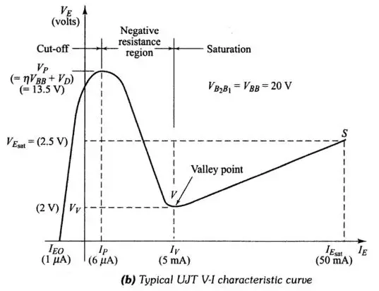
When the VE-IE is shows that IE for positive close the peak point P, when VE absolutely equal VP the emitter equal Ip, the peak point current. At this point, holes from the heavily doped emitter are injected into the N- layer substrate, usually into the B1 region. The substrate which is lightly doped, provide very little chance for these holes to recombine. As like as the lower of the substrate for replete with additional current carriers (holes) and its resistance RB1 is drastically reduced. The decrease in RB1 due to Vx to drop. This drop in turn due to the diode to become more forward biased, and IE increases even further. The larger IE delivers more holes B1, and reducing RB1.This regeneration or snowballing process ends, RB1 has dropped to a very small value (2-25Ω) and IE can become large and limited RE .
Output waveform for UJT
The device has switched to the low voltage, high current region of its VE – IE. The slanding line of this on portions is leakage and mentioned resistance value is low, in this area , the emitter voltage VE, will be compared small and naturally 2V and remains equability steady state as IE is raised up to its higher range value of IE –saturation. Consequently at one time the device is raising VEE will delivers and to increase IE although VE remains closed to near 2V.
The device gets triggered at one time the UJTs emitter current based on major VEE and RE . As VEE decreases and IE will decrease along the on portion of the VE – IE loop. When IE decrease to point V, the valley point , and the emitter current is equal to IV , the valley current , which is essentially the holding current needed to keep the UJT on. when IE decreased below IV , the UJT turns off and its operation rapidly switches back to the off region of its VE – IE curve, where IE ≈ 0 and VE – VEE. The valley current is the counterpart of the holding current in PNPN devices, and generally ranges between 1 and 10mA.
Example For UJT:
2N2646, is a Unijunction (UJT) Transistor, 2 A, 1 µA, 6 mA, TO-18, 3 Pin, 125 °C
Rate: 5 USD or 390 INR